Semiconductor Packaging Adhesive Manufacturer
Flip chip underfill · Die attach · SiP adhesive · Optical bonding — engineered to eliminate
defects holding back your 2.5D/3D packaging yield.
Advanced semiconductor packaging demands tighter tolerances. These are the defects
that kill yield — and how our underfill and adhesive materials solve them.
From warpage in thin substrates to void formation during underfill dispensing, these are the defects that hold back 2.5D/3D packaging yield. COFA materials are formulated to address each one.
CTE mismatch causes die and substrate warpage. Our low-shrinkage formulations minimize thermal stress.
Trapped air during dispensing leads to reliability failure. Optimized flow and wetting properties eliminate voids.
Thermal shock causes interface separation. High-adhesion epoxy systems ensure bond integrity across temperature cycles.
Long cure times reduce throughput. Fast-cure options (80°C / 30min) accelerate your production cycle.
11+ flip chip underfill, die attach, and SiP adhesive formulations across three cure technologies, filterable by viscosity and application.
High-flowability underfill for fine-pitch flip-chip & HBM. Minimizes CTE mismatch stress and warpage in 2.5D/3D packages.
Heat-resistant underfill with controlled flow for demanding environments. Prevents delamination under extreme thermal cycling.
Balanced viscosity with high toughness. Ideal for packages requiring void-free fill and mechanical durability.
Fast cure at 80°C / 30min for board-level reinforcement. Reduces process time without compromising adhesion strength.
High hardness board reinforcement adhesive. Strong substrate bonding with minimal voiding under thermal stress.
Low-stress die attach adhesive. Absorbs thermal expansion mismatch to prevent warpage in thin die assemblies.
Low-viscosity die attach variant for ultra-low stress applications. Minimizes warpage in thin die-bonded packages.
Dual-cure adhesive for camera and sensor modules. High toughness prevents delamination under drop and thermal shock.
Low-viscosity UV-curable adhesive with excellent optical clarity. Zero voiding for precision optical assembly.
Medium-viscosity UV-curable adhesive. Controlled flow prevents overflow in tight optical bond lines.
Optimized for thin and delicate structures. Uniform bond line with minimal thermal stress during UV cure.
Technical specifications for our most adopted products. Request a TDS for full evaluation data.
From FCBGA flip chip underfill to SiP adhesive and camera module bonding.
Void-free capillary underfill for fine-pitch 2.5D/3D packages
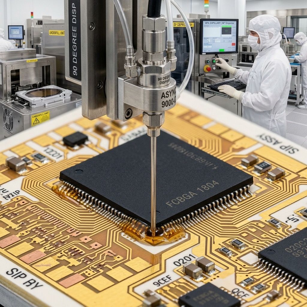
Reliable FCBGA underfill for high-bandwidth memory stacks
Drop-resistant bonding for mobile image sensors
UV-cure bonding with optical clarity
Fast-cure reinforcement for PCB-level reliability
Die attach & underfill for multi-chip stacking
Multi-function integration with reliable SiP adhesive bonding
Layer-stacked packaging with controlled underfill flow
COFA is an epoxy resin-based adhesive company focused on semiconductor and electronics packaging.
With over two decades of formulation experience, we develop adhesive materials tailored to your specific packaging process — from resin design and filler dispersion to cure optimization.
Our lineup covers flip-chip underfill, die attach, optical bonding, and board reinforcement. All formulated and produced in Korea, validated in real production environments.
COFA established to bring 20+ years of adhesive formulation expertise into semiconductor packaging.
First underfill and adhesive formulations developed. Core technology platform for epoxy-based systems established.
Materials qualified and adopted by production clients. Full lineup of 11+ formulations completed.
Expanding into global semiconductor packaging market with an extended product portfolio and customer base.
Perspectives on semiconductor packaging, adhesive technology, and industry trends.
Full 3D stacking with HBM and TSV remains the domain of tier-1 players like SK Hynix and Samsung.
But for most semiconductor companies, the realistic entry point is 2-layer stacking with flip-chip architecture.
At this stage, flip-chip underfill becomes the critical enabler: protecting micro-bumps, distributing thermal stress,
ensuring long-term reliability, and surviving repeated temperature cycles in mobile environments.
As AI moves on-device with NPUs and edge computing, mobile devices are becoming small data centers.
Even 2-layer stacking significantly reduces data travel distance and latency.
The competition isn't about who stacks the most transistors.
It's about who can implement stacking at a realistic level and keep it stable.
Adhesive materials sit at the center of that question.
As NPU and edge computing push into mobile, even 2-layer stacking changes the game. Data travel distance drops, latency drops, and real performance goes up.
Connecting heterogeneous materials reliably, managing heat and stress at micro-scale, and ensuring long-term durability. This is what packaging adhesives do.
Moore's law is hitting physical limits. The answer is stacking, chiplets, and advanced packaging. And at the foundation of all of it is materials technology.
Samples, technical data, or general questions. We respond within one business day.